Chen Jianping and Zhou Linjie's research group:
Optical buffer has attained distinguished achievement
In the information age, the Internet has developed rapidly. Communication networks have greatly promoted the development of data centers. Currently, copper cables are still widely used in data center cabinets, but existing data transmission technologies will soon reach performance limits, such as bandwidth and cost. Power consumption, etc. It is an inevitable trend for the optical field to enter and exit in the field of interconnection. Optical interconnect technology continues to expand from long distances to short distances, which requires optical devices to move toward high speed, small size, and low power consumption. Integrated photonic devices are the best choice for on-chip optical interconnects due to their small size, low power consumption, and good stability. Silicon materials are the most widely used materials in integrated circuits due to their superior semiconductor properties and stable, mature fabrication processes. Silicon-based photonic devices have their unique technological advantages, including higher integration than traditional optoelectronic devices, more features to embed, lower power consumption and higher reliability, making them one of the hottest research topics in integrated optics today.
Data caching is a key module in optical communication networks. It can avoid channel network conflicts and improve node throughput and reduce packet loss rate. Performance metrics for data caching are more demanding in next-generation all-optical switching networks such as packet switching. Early all-optical switching networks used electrical random access memory (RAM) to access information. The optical switching speed of this method is limited by the reading speed of the electrical RAM, and the scheme must be converted by photoelectric light. The system is more complicated, and the electrical power consumption of the system is also relatively large. Therefore, people began to think about whether it is possible to complete the data buffer function directly in the optical system without photoelectric photoelectric conversion. Unfortunately, there is no mature optical storage solution or device. Therefore, the existing data cache and synchronization functions are available. The optical system is implemented by a variety of tunable optical buffers. Optical buffer can achieve accurate synchronization of multi-channel signals and solve data competition conflicts. It is an essential component for building a future all-optical switching network.

Figure 1 (a) Schematic diagram of cascaded microring delay line; (b) Schematic diagram of reconfigurable optical delay line
There are two ways to implement optical caching. One is to reduce the group velocity of light by a ring resonator, a photonic crystal, a Bragg grating, etc. (Fig. 1a). Among them, the ring resonator has the advantages of compact structure and simple structure, and can change the group speed by moving the wavelength of the resonance point, thereby achieving continuous adjustment of the group delay. The other is to achieve different time delays by adjusting the length of the path through which the light passes (Fig. 1b). Professor Chen Jianping, the regional key laboratory of the regional optical fiber communication network and the new optical communication system of Shanghai Jiaotong University, under the leadership of Professor Zhou Linjie, the "Seven-bit reconfigurable optical true time delay line based on silicon integration" Highlights of Nature Photonics. This scheme can be used to implement continuous large-scale reconfigurable delay lines, but limited by the length required to accurately calculate and the shortest length value (minimum delay increment), can not achieve high precision delay.
In the research process of the mechanism and key technologies of silicon-based optical delay lines, there are mainly the following problems that need to be overcome: (1) how to achieve a larger delay adjustment range and higher adjustment accuracy; (2) how to Reduce device insertion loss; (3) How to reduce regulation power consumption; (4) How to perform electrical and optical packaging.
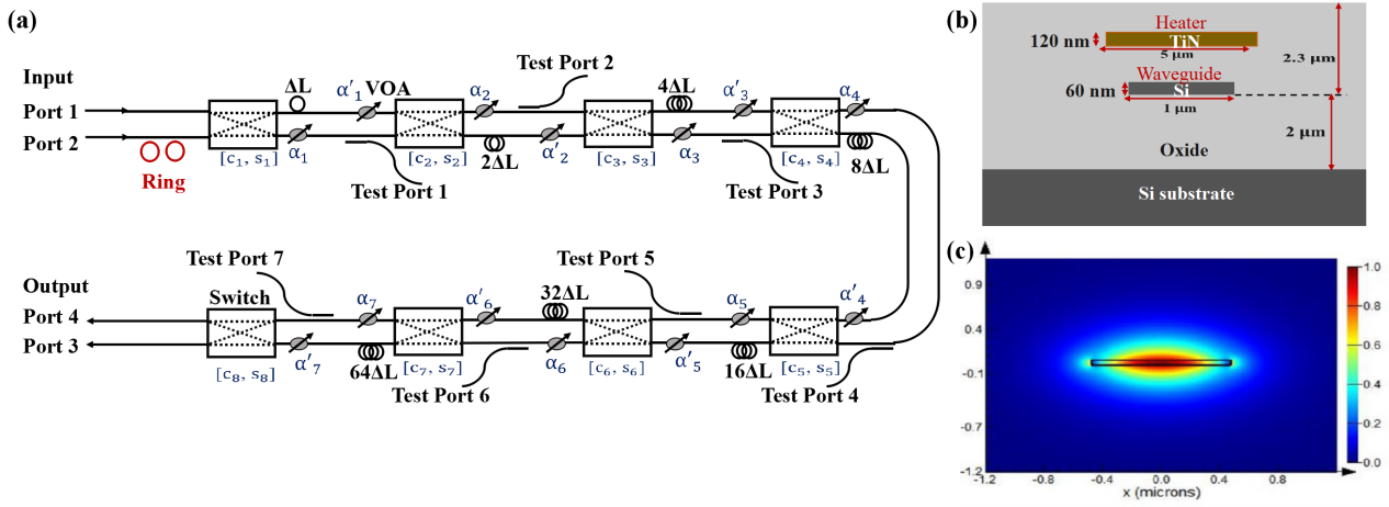
Figure 2 (a) Schematic diagram of the continuously dimmable delay line; (b) the cross section of the ultrathin waveguide; (c) the electric field distribution of the fundamental mode
In 2017, under the leadership of Professor Zhou Linjie, a cascaded ring resonator and a reconfigurable delay network were combined to propose and implement a silicon-based continuous wide-range adjustable optical buffer chip (Fig. 2a). In response to the current problems, the research team proposed and implemented the following schemes: (1) combining the cascaded ring resonator with the reconfigurable delay network to achieve wide-range continuous adjustment; (2) using 60nm thin The silicon waveguide replaces the ridge waveguide structure (Fig. 2b-c). Since the thin silicon waveguide has a strong binding ability to light, the use of a thin silicon waveguide can effectively reduce the transmission loss of light. (3) The proposed cascaded Mach-Zehnder switch structure eliminates the need to turn on the adjustable attenuator to reduce power consumption. (4) The metal pad wire in the chip is bonded to the PCB board, and the fiber array and the chip are fixed by UV glue, and the whole chip is packaged.
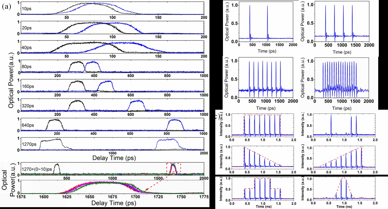
Figure 3 (a) Continuous dimming delay test chart; (b) Time division multiplexing test chart; (c) Arbitrary waveform generation chart
In this work, the research team proved through experiments: (1) The adjustable delay amount of the ring delay line is greater than 10ps, combined with the 7-bit reconfigurable optical delay line with an adjustment accuracy of 10ps, which can achieve 0. -1.28 ns continuously adjustable (Fig. 3a); (2) Optical buffer chip based on ultra-thin silicon waveguide platform, the loss is only 12.4 dB at a maximum delay of 1.28 ns; (3) π required for each optical switch The phase shift power consumption is only 10mW. Compared with the single Mach-Zehnder structure, the new two-stage cascaded Mach-Zehnder structure is used as the switching unit, which improves the extinction ratio of the switch, and the extinction ratio reaches 25dB in the range of 1520nm to 1580nm. The two-stage cascade switch is used as the switch unit of the 7-bit adjustable delay line, which greatly reduces the crosstalk of the signal. Therefore, the signal quality can be ensured without opening the tunable optical attenuator, so that the complexity of the structure and the overall power consumption are significantly reduced. (4) The chip has functions such as optical time division multiplexing (Fig. 3b), arbitrary waveform generation (Fig. 3c) and filtering. These functions can be controlled by the circuit system.
Compared with the highest international level, the optical buffer chip of the research group has superior performance indicators such as low loss, wide range continuous adjustment, high stability, high resolution and high tuning efficiency. The chip integrates dozens of electrical and optical components such as microring resonators, Mach-Zehnder interferometer switches, tunable optical attenuators, micro-heaters, grating couplers and more. These components are integrated on a silicon photonic chip and CMOS process compatible, greatly improving the performance of optoelectronic chips and laying the foundation for large-scale, low-cost production.
Optical buffers are also widely used in the field of microwave photons, such as light-controlled phased array radars and microwave photonic filters. In the traditional electrical phased array radar, since the phase shift amount of the microwave phase shifter is independent of the frequency, the direction angles corresponding to the microwave signals of different frequencies are inconsistent and the aperture effect is introduced. The phase shifter unit in the optically controlled phased array radar realized by the optical system adopts the dimmable delay line, and puts forward higher requirements on the adjustment range and accuracy, and can overcome the aperture caused by the limited bandwidth of the electronic phase shifter. The phenomenon of crossing is one of the key technologies in the new system radar.